Hardware Security
Security Heading link
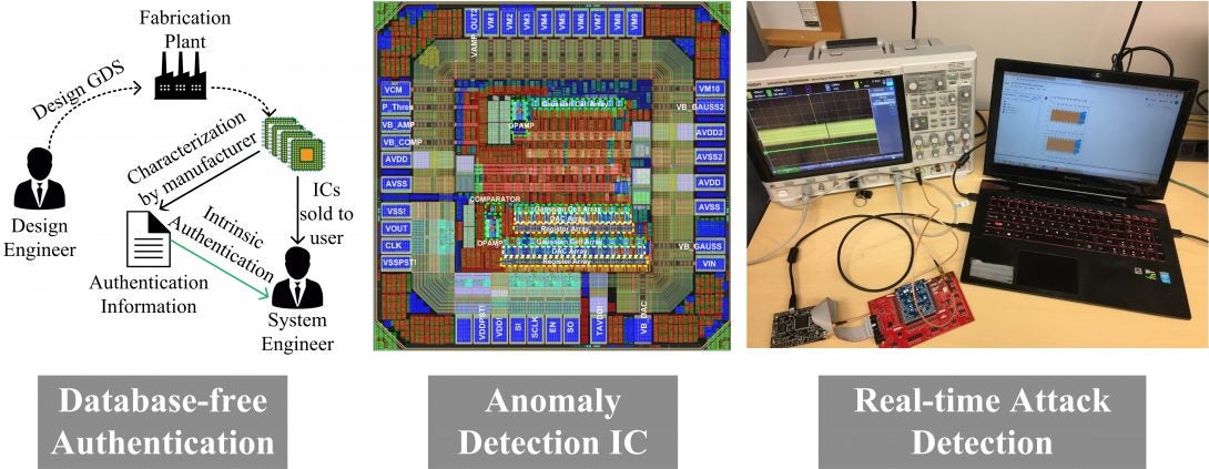
Edge devices can have complicated long life and origin, therefore, are highly vulnerable to diverse security issues during system integration and field operation. Current state-of-the-art authentication protocols rely on Physically Unclonable Functions (PUF). PUF is a unique circuit module to generate an unclonable and unpredictable fingerprint for each chip. Authentication protocols then enroll unique fingerprints for each legitimate IC to a centralized database, which is used to verify the authenticity of ICs. However, such an authentication scheme has several drawbacks. First, PUFs have considerable area/power overhead, causing considerable challenges to integrating them within area/power-constrained edge devices. Secondly, PUFs increase test workload to create a database of challenge-response (CR) pairs for each IC, which adds to the test cost and makes a trust concern since most fabless companies rely on third-party (often untrusted) test facilities.
To address this critical challenge, we developed an authentication protocol that comes at virtually zero design overhead and minimal test/characterization cost for the chip manufacturers. Our authentication solution eliminated the need to enroll and maintain valid chip signatures in a database, resulting in a database-free authentication. Our framework transformed inherent variations in circuit parameters (e.g., scan path delays, memory reliability map, analog parameters) into robust signatures (i.e., watermark) through parametric measurements and statistical analysis on a small unit of authentic chips. Such a watermark is a joint function of a chip layout, process, foundry, and package (for analog components) and hence, is highly sensitive to any change in one or more of these conditions. Thus, a counterfeit chip (e.g., a cloned or remarked one) can be isolated with high accuracy. Second, we extended the scheme to generate a unique identifier for each chip, when needed, using built-in circuit structures (e.g., scan chain). Third, we developed a secure communication protocol such that in-field integrity violations (e.g., replacing an authentic chip with a fake one) can be detected during an IoT device’s lifetime. Our research led to several key publications in top IEEE journals and conferences. Semiconductor Research Corporations funded this research.
Key Publications:
- Ahish Shylendra, Priyesh Shukla, Saibal Mukhopadhyay, Swarup Bhunia, and Amit Ranjan Trivedi. “Low Power Unsupervised Anomaly Detection by Nonparametric Modeling of Sensor Statistics.” IEEE Transactions on Very Large Scale Integration (VLSI) Systems, 2020.
- Ahish Shylendra, Priyesh Shukla, Swarup Bhunia, and Amit Ranjan Trivedi. “Fault attack detection in AES by monitoring power side-channel statistics.” In IEEE International Symposium on Quality Electronic Design (ISQED), 2020.
- Ahish Shylendra, Swarup Bhunia, and Amit Ranjan Trivedi. “An Intrinsic and Database-Free Authentication by Exploiting Process Variation in Back-End Capacitors.” IEEE Transactions on Very Large Scale Integration (VLSI) Systems, 2019.
- Ahish Shylendra, Swarup Bhunia, and Amit Ranjan Trivedi “Intrinsic and Database-free Watermarking in ICs by Exploiting Process and Design Dependent Variability in Metal-Oxide-Metal Capacitances,” IEEE/ACM International Symposium on Low Power Electronics and Design (ISLPED), 2018.